Sunday, November 30, 2008

Mattel Children's Hospital UCLA launches program in nanopediatrics

Edward R.B. McCabe, MD

Edward R.B. McCabe, MD Physician-in-Chief, Mattel Children's Hospital UCLA and Executive Chair, UCLA Department of Pediatrics
Program to explore use of nanotechnology in diagnostics, treatment

Mattel Children's Hospital UCLA today announced the launch of the Mattel UCLA NanoPediatrics Program, which will explore the future of personalized medicine for children, including the opportunities and risks involved. The program is one of the world's first dedicated solely to nanomedicine and pediatric patients.

"Why develop a nanopediatrics program? Because children are not small adults," said Dr. Edward McCabe, physician-in-chief of Mattel Children's Hospital and founding director of the new program. "We know that drugs affect children — they metabolize, excrete and may even utilize, developmentally, specific receptors — differently than adults.
"Unless children are included as a research priority for the application of nanotechnology, then we will simply be applying approaches developed for adults. This flawed strategy will place children at risk, as opposed to a program in which children will be the focus from the outset."

Nanotechnology involves manipulating atoms and molecules to create tiny devices, smaller than one-thousandth the diameter of a human hair (a nanometer is one-billionth of a meter). It is anticipated that nanomedicine, fueled by nanotechnology, will enable more personalized medical care that will be both predictive and preventive.

While considerable attention has been paid to nanomedicine, UCLA's nanopediatrics program, initially organized in May 2008, may be the first initiative to examine the promises and risks of nanodiagnostics and nanotherapeutics for children in a formal and organized manner.

Created thanks to a generous $1.8 million gift from the Mattel Children's Foundation, the program will support a nanopediatrics research core and pilot funding for projects that will potentially enable investigators to obtain grants from the National Institutes of Health.

"The Mattel Children's Foundation is excited to support this groundbreaking program in nanopediatrics, which can potentially revolutionize the research and treatment of illnesses that affect young patients," said Kevin Farr, chairman of the foundation and chief financial officer of Mattel Inc. "Our philanthropic vision is to make a meaningful difference, one child at a time, and we believe that the nanopediatrics program at Mattel Children's Hospital UCLA will bring new technologies and treatments to better the lives of children battling for their health."

Projects currently underway at UCLA include the development and application of nanodiagnostic tools such as DNA-based newborn screening tests for genetic abnormalities, the development of a new generation of nanodevices for the treatment of children with genetic diseases and cancer, and the investigation of the use of nanoparticles for diagnostic imaging both during pregnancy and after birth.

The Mattel UCLA NanoPediatrics Program will partner with the California NanoSystems Institute (CNSI) at UCLA, an integrated research center established in 2000 to encourage university collaboration with industry and enable the rapid commercialization of discoveries in nanosystems. For additional information, visit www.nanopediatrics.ucla.edu. ###

Contact: Amy Albin aalbin@mednet.ucla.edu 310-794-8672 University of California - Los Angeles

Tags: or and

Saturday, November 29, 2008

New solar energy material captures every color of the rainbow

Malcolm Chisholm

Malcolm Chisholm
COLUMBUS, Ohio -- Researchers have created a new material that overcomes two of the major obstacles to solar power: it absorbs all the energy contained in sunlight, and generates electrons in a way that makes them easier to capture.

Ohio State University chemists and their colleagues combined electrically conductive plastic with metals including molybdenum and titanium to create the hybrid material.
"There are other such hybrids out there, but the advantage of our material is that we can cover the entire range of the solar spectrum," explained Malcolm Chisholm, Distinguished University Professor and Chair of the Department of Chemistry at Ohio State.

The study appears in the current issue of the Proceedings of the National Academy of Sciences (PNAS).

Sunlight contains the entire spectrum of colors that can be seen with the naked eye -- all the colors of the rainbow. What our eyes interpret as color are really different energy levels, or frequencies of light. Today's solar cell materials can only capture a small range of frequencies, so they can only capture a small fraction of the energy contained in sunlight.

This new material is the first that can absorb all the energy contained in visible light at once.

The material generates electricity just like other solar cell materials do: light energizes the atoms of the material, and some of the electrons in those atoms are knocked loose.

Ideally, the electrons flow out of the device as electrical current, but this is where most solar cells run into trouble. The electrons only stay loose for a tiny fraction of a second before they sink back into the atoms from which they came. The electrons must be captured during the short time they are free, and this task, called charge separation, is difficult.

In the new hybrid material, electrons remain free much longer than ever before.

To design the hybrid material, the chemists explored different molecular configurations on a computer at the Ohio Supercomputer Center. Then, with colleagues at National Taiwan University, they synthesized molecules of the new material in a liquid solution, measured the frequencies of light the molecules absorbed, and also measured the length of time that excited electrons remained free in the molecules.

They saw something very unusual. The molecules didn't just fluoresce as some solar cell materials do. They phosphoresced as well. Both luminous effects are caused by a material absorbing and emitting energy, but phosphorescence lasts much longer.

To their surprise, the chemists found that the new material was emitting electrons in two different energy states -- one called a singlet state, and the other a triplet state. Both energy states are useful for solar cell applications, and the triplet state lasts much longer than the singlet state.

Electrons in the singlet state stayed free for up to 12 picoseconds, or trillionths of a second -- not unusual compared to some solar cell materials. But electrons in the triplet state stayed free 7 million times longer -- up to 83 microseconds, or millionths of a second.

When they deposited the molecules in a thin film, similar to how they might be arranged in an actual solar cell, the triplet states lasted even longer: 200 microseconds.

"This long-lived excited state should allow us to better manipulate charge separation," Chisholm said.

At this point, the material is years from commercial development, but he added that this experiment provides a proof of concept -- that hybrid solar cell materials such as this one can offer unusual properties.

The project was funded by the National Science Foundation and Ohio State's Institute for Materials Research.

Chisholm is working with Arthur J. Epstein, Distinguished University Professor of chemistry and physics; Paul Berger, professor of electrical and computer engineering and physics; and Nitin Padture, professor of materials science and engineering to develop the material further. That work is part of the Advanced Materials Initiative, one Ohio State's Targeted Investment in Excellence (TIE) programs.

The TIE program targets some of society's most pressing challenges with a major investment of university resources in programs with a potential for significant impact in their fields. The university has committed more than $100 million over the next five years to support 10 high-impact, mostly interdisciplinary programs.

Co-authors on the PNAS paper from Ohio State included: Gotard Burdzinski, a postdoctoral researcher; Yi-Hsuan Chou, a postdoctoral researcher; Florian Fiel, a former postdoctoral researcher; Judith Gallucci, a senior research associate; Yagnaseni Ghosh, a graduate student; Terry Gustafson, a professor; Yao Liu, a postdoctoral researcher; Ramkrishna Ramnauth, a former postdoctoral researcher; and Claudia Turro, a professor; all of the Department of Chemistry. They collaborated with Pi-Tai Chou and Mei-Lin Ho of National Taiwan University.

Contact: Malcolm Chisholm, (614) 292-7216; Chisholm.4@osu.edu
Written by Pam Frost Gorder, (614) 292-9475; Gorder.1@osu.edu
WEB: Ohio State University

Tags: or and

Friday, November 28, 2008

New research field promises radical advances in optical technologies

Numerical Simulations

These are graphical representations of numerical simulations depicting four potential applications of a new field called transformation optics. Clockwise from top left are: a design for optical cloaking; a light "concentrator" for sensors and solar collectors; a "planar hyperlens" and "impedence-matched hyperlens" for applications including microscopes. (Courtesy of the journal Science) Usage Restrictions: None.
WEST LAFAYETTE, Ind. - A new research field called transformation optics may usher in a host of radical advances including a cloak of invisibility and ultra-powerful microscopes and computers by harnessing nanotechnology and "metamaterials."

The field, which applies mathematical principles similar to those in Einstein's theory of general relativity, will be described in an article to be published Friday (Oct. 17) in the journal Science. The article will appear in the magazine's Perspectives section and was written by Vladimir Shalaev, Purdue's Robert and Anne Burnett Professor of Electrical and Computer Engineering.
The list of possible breakthroughs includes a cloak of invisibility; computers and consumer electronics that use light instead of electronic signals to process information; a "planar hyperlens" that could make optical microscopes 10 times more powerful and able to see objects as small as DNA; advanced sensors; and more efficient solar collectors.

"Transformation optics is a new way of manipulating and controlling light at all distances, from the macro- to the nanoscale, and it represents a new paradigm for the science of light," Shalaev said. "Although there were early works that helped to develop the basis for transformation optics, the field was only recently established thanks in part to papers by Sir John Pendry at the Imperial College, London, and Ulf Leonhardt at the University of St. Andrews in Scotland and their co-workers."

Current optical technologies are limited because, for the efficient control of light, components cannot be smaller than the size of the wavelengths of light. Transformation optics sidesteps this limitation using a new class of materials, or metamaterials, which are able to guide and control light on all scales, including the scale of nanometers, or billionths of a meter.

"The whole idea behind metamaterials is to create materials designed and engineered out of artificial atoms, meta-atoms, which are smaller than the wavelengths of light itself," Shalaev said. "One of the most exciting applications is an electromagnetic cloak that could bend light around itself, similar to the flow of water around a stone, making invisible both the cloak and an object hidden inside."

Shalaev and researchers from his group - doctoral students Wenshan Cai and Uday K. Chettiar and principal research scientist Alexander V. Kildishev - in 2007 took a step toward creating an optical cloaking device in the visible range of the spectrum. Their theoretical design uses an array of tiny needles radiating outward from a central spoke, resembling a round hairbrush, and would bend light around the object being cloaked.

The mathematical equations for transformation optics are similar to the mathematics behind Einstein's theory of general relativity, which describes how gravity warps space and time, Shalaev said.

"Whereas relativity demonstrates the curved nature of space and time, we are able to curve space for light, and we can design and engineer tiny devices to do this," he said. "In addition to curving light around an object to render it invisible, you could do just the opposite - concentrate light in an area, which might be used for collecting sunlight in solar energy applications. So, general relativity may find practical use in a number of novel optical devices based on transformation optics."

The metamaterials also may enable engineers to overcome obstacles now confronting the semiconductor industry: It is becoming increasingly difficult to make faster computer chips because the technology is reaching its limits. But computers using light instead of electronic signals to process information would be thousands of times faster than conventional computers. Such "photonic" computers would contain special transistor-size optical elements made from metamaterials.

Transformation optics also could enable engineers to design and build a "planar magnifying hyperlens" that would drastically improve the power and resolution of light microscopes.

"The hyperlens is probably the most exciting and promising metamaterial application to date," Shalaev said. "The first hyperlens, proposed independently by Evgenii Narimanov at Princeton and Nader Engheta at the University of Pennsylvania and their co-workers, was cylindrical in shape. Transformation optics, however, enables a hyperlens in a planar form, which is important because you could just simply add this flat hyperlens to conventional microscopes and see things 10 times smaller than now possible. You could focus down to the nanoscale, much smaller than the wavelength of light, to actually see molecules like DNA, viruses and other objects that are now simply too small to see."

The hyperlens theoretically would compensate for the loss of a portion of the light transmitting fine details of an image as it passes through a lens. Lenses and imaging systems could be improved if this lost light, which scientists call "evanescent light," could be restored. Such a hyperlens would both magnify an image and convert this evanescent light so that it does not weaken with distance but continues to propagate.

Meta in Greek means beyond, so the term metamaterial means to create something that doesn't exist in nature.

Unlike natural materials, metamaterials are able to reduce the "index of refraction" to less than one or less than zero. Refraction occurs as electromagnetic waves, including light, bend when passing from one material into another. It causes the bent-stick-in-water effect, which occurs when a stick placed in a glass of water appears bent when viewed from the outside. Each material has its own refraction index, which describes how much light will bend in that particular material and defines how much the speed of light slows down while passing through a material.

Natural materials typically have refractive indices greater than one. Metamaterials, however, can make the index of refraction vary from zero to one, which possibly will enable cloaking as well as other advances, Shalaev said.

He estimated that researchers may be building prototypes using transformation optics, such as the first planar hyperlenses, within five years. ###

Various research groups around the world are working in transformation optics. The U.S. Office of Naval Research and Department of Defense are creating a new multidisciplinary university research initiative, or MURI, to fund work in the field. MURIs are collaborative efforts among researchers at several universities, but the participants have not yet been selected.

Shalaev's research is based at the Birck Nanotechnology Center at Purdue's Discovery Park. The research is funded by the U.S. Army Research Office.

Writer: Emil Venere, (765) 494-4709, venere@purdue.edu, Source: Vladimir Shalaev, (765) 494-9855, shalaev@ecn.purdue.edu

Related Web site: Vladimir Shalaev: engineering.purdue.edu/ECE/People/profile

Note to Journalists: A copy of the research paper is available by contacting the Science Press Package team at (202) 326-6440, scipak@aaas.org

Contact: Emil Venere venere@purdue.edu 765-494-4709 Purdue University

Tags: or and

Thursday, November 27, 2008

First tunable, 'noiseless' amplifier may boost quantum computing, communications

Noiseless Amplifier

Caption: In the JILA/NIST "noiseless" amplifier, a long line of superconducting magnetic sensors (beginning on the right in this photograph) made of sandwiches of two layers of superconducting niobium with aluminum oxide in between, creates a "metamaterial" that selectively amplifies microwaves based on their amplitude rather than phase.

Credit: M. Castellanos-Beltran/JILA. Usage Restrictions: None.
Researchers at the National Institute of Standards and Technology (NIST) and JILA, a joint institute of NIST and the University of Colorado (CU) at Boulder, have made the first tunable “noiseless” amplifier. By significantly reducing the uncertainty in delicate measurements of microwave signals, the new amplifier could boost the speed and precision of quantum computing and communications systems.

Conventional amplifiers add unwanted “noise,” or random fluctuations, when they measure and boost electromagnetic signals.
Amplifiers that theoretically add no noise have been demonstrated before, but the JILA/NIST technology, described in an Oct. 5, 2008, advance online publication of Nature Physics,* offers better performance and is the first to be tunable, operating between 4 and 8 gigahertz, according to JILA group leader Konrad Lehnert. It is also the first amplifier of any type ever to boost signals sufficiently to overcome noise generated by the next amplifier in a series along a signal path, Lehnert says, a valuable feature for building practical systems.

Noisy amplifiers force researchers to make repeated measurements of, for example, the delicate quantum states of microwave fields—that is, the shape of the waves as measured in amplitude (or power) and phase (or point in time when each wave begins). The rules of quantum mechanics say that the noise in amplitude and phase can’t both be zero, but the JILA/NIST amplifier exploits a loophole stipulating that if you measure and amplify only one of these parameters—amplitude, in this case—then the amplifier is theoretically capable of adding no noise. In reality, the JILA/NIST amplifier adds about half the noise that would be expected from measuring both amplitude and phase.

The JILA/NIST amplifier could enable faster, more precise measurements in certain types of quantum computers—which, if they can be built, could solve some problems considered intractable today—or quantum communications systems providing “unbreakable” encryption. It also offers the related and useful capability to “squeeze” microwave fields, trading reduced noise in the signal phase for increased noise in the signal amplitude. By combining two squeezed entities, scientists can “entangle” them, linking their properties in predictable ways that are useful in quantum computing and communications. Entanglement of microwave signals, as opposed to optical signals, offer some practical advantages in computing and communication such as relatively simple equipment requirements, Lehnert says.

The new amplifier is a 5-millimeter-long niobium cavity lined with 480 magnetic sensors called SQUIDs (superconducting quantum interference devices). The line of SQUIDs acts like a “metamaterial,” a structure not found in nature that has strange effects on electromagnetic energy. Microwaves ricochet back and forth inside the cavity like a skateboarder on a ramp. Scientists tune the wave velocity by manipulating the magnetic fields in the SQUIDs and the intensity of the microwaves. An injection of an intense pump tone at a particular frequency, like a skateboarder jumping at particular times to boost speed and height on a ramp, causes the microwave power to oscillate at twice the pump frequency. Only the portion of the signal which is synchronous with the pump is amplified. ###

Funding for the research was provided by NIST, the National Science Foundation, and a NIST-CU seed grant.

* M.A. Castellanos-Beltran, K.D. Irwin, G.C. Hilton, L.R. Vale and K.W. Lehnert. Amplification and squeezing of quantum noise with a tunable Josephson metamaterial. Nature Physics, published online: 5 Oct. 5 2008; doi:10.1038/nphys1090.

Contact: Laura Ost laura.ost@nist.gov 303-497-4880 National Institute of Standards and Technology (NIST)

Tags: or and

Wednesday, November 26, 2008

Gold nanostars outshine the competition

Gold Nanostars Outshine the Competition

Caption: NIST scientists found that gold and silver nanostars improved the sensitivity of Surface Enhanced Raman Spectroscopy 10 to 100,000 times that of other commonly used nanoparticles. These uniquely shaped nanoparticles may one day be used in a range of applications from disease diagnostics to contraband identification. Color added for clarity.

Credit: NIST. Usage Restrictions: None.
Novel nanoparticles being tested at the National Institute of Standards and Technology (NIST) have researchers seeing stars. In a recent paper,* NIST scientists used surface-enhanced Raman spectroscopy (SERS) to demonstrate that gold nanostars exhibit optical qualities that make them superior for chemical and biological sensing and imaging. These uniquely shaped nanoparticles may one day be used in a range of applications from disease diagnostics to contraband identification.
SERS relies on metallic nanoparticles, most commonly gold and silver, to amplify signals from molecules present in only trace quantities. For these types of experiments, scientists shine laser light on an aqueous solution containing the nanoparticles and the molecule of interest and monitor the scattered light. The detailed characteristics of both the molecule and the nanoparticle affect the strength of scattered light, which contains an identifying fingerprint for the molecule known as its vibrational signature. With nanoparticles amplifying the signature, it is possible to detect a very low concentration of molecules in a solution.

The NIST team tested the optical properties of the nanostars using two target molecules, 2-mercaptopyridine and crystal violet. These molecules were selected because of their structural similarity to biological molecules and their large number of delocalized electrons, a characteristic that lends itself to SERS. NIST researchers found that the Raman signal of 2-mercaptopyridine was 100,000 stronger when nanostars were present in the solution. The stars were also shown to be particularly capable of enhancing the signature of crystal violet, delivering a signal about 10 times stronger than the previous winner, nanorods. Both the nanostars and the nanorods outperformed the nanospheres commonly used for Raman enhancement.

NIST physicist Angela Hight Walker and her team perfected the process for making gold nanostars, building them from the bottom-up using surface alterations to manipulate their growth and control their shape. Once suspended in a solution, the team guided the nanostars to gather together to form multiple “hot spots,” where the enhancement is dramatically larger than for a single nanostar.

According to Hight Walker, the fact that they can now be created en masse and have desirable optical properties should prompt researchers to examine their possible applications, perhaps eventually making them the stars of the nanoworld. ###

* E. Nalbant Esenturk and A. R. Hight Walker. Surface-enhanced Raman scattering spectroscopy via gold nanostars. Journal of Raman Spectroscopy, published online Sept. 24, 2008, DOI: 10.1002/jrs.2084.

Contact: Mark Esser mark.esser@nist.gov 301-975-8735 National Institute of Standards and Technology (NIST)

Tuesday, November 25, 2008

Paperwork: Buckypapers clarify electrical, optical behavior of nanotubes

Buckypapers Clarify Electrical, Optical Behavior of Nanotubes

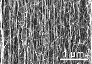
Caption: Buckypaper: SEM image demonstrates a pseudo 2-D network of carbon nanotubes deposited like paper fibers in a thin, sparse sheet. The nanotubes here have an average length 820 nm and make a continuous, electrically conducting network overall in spite of obvious gaps. On a macroscale this material would be nearly transparent. Color added for clarity

Credit: Chastek/Talbott NIST. Usage Restrictions: None.
Using highly uniform samples of carbon nanotubes—sorted by centrifuge for length—materials scientists at the National Institute of Standards and Technology (NIST) have made some of the most precise measurements yet of the concentrations at which delicate mats of nanotubes become transparent, conducting sheets. Their recent experiments* point up the importance of using relatively homogeneous—not overly short, but uniform in length— nanotubes for making high performance conducting films.

Among their other qualities, single-wall carbon nanotubes (SWCNTs) have attracted much attention as tiny electrical conductors.
Relatively small concentrations of nanotubes can change a normally insulating polymer film to a transparent electrical conductor. Potential applications range from transparent electrical shielding materials to futuristic flexible video displays, thin-film chemical sensors and other foldable electronics. One key design parameter for conductive films is the so-called “percolation threshold”—essentially the concentration at which random two- or three-dimensional networks of nanotubes first become electrically conducting.

To test theories on how both the conductance and optical properties of such nanotube-infused films depend on the length of the tubes, the NIST team made samples of “buckypaper” by mixing nanotubes in water and draining the water away through nanoscale filters to leave behind a delicate nanotube mat. The highly refined, length-sorted nanotube samples were produced by an efficient technique developed earlier by the NIST group (see “Spin Control: New Technique Sorts Nanotubes by Length”).

The NIST measurements validated one theory: buckypaper made of length-sorted carbon nanotubes closely follows the percolation theory for ideal two-dimensional sheets, with concentration threshold for conductivity getting lower as the tubes get longer. A sheet of 820 nanometer long nanotubes becomes conducting at an amazingly low 18 nanograms per square centimeter, the lowest yet reported. Interestingly, batches of short nanotubes or mixed-length batches form more three-dimensional networks that perform noticeably worse. On the other hand, predictions that optically the sheets would behave like thin metallic films turn out not to be the case. Optical properties are better predicted by the same general percolation theory, say the NIST researchers, which will provide a convenient theoretical framework for designing and engineering nanotech applications with these materials. ###

* D. Simien, J.A. Fagan, W. Luo, J.F. Douglas, K. Migler and J. Obrzut. Influence of nanotube length on the optical and conductivity properties of thin single-wall carbon nanotube networks. ACS Nano, Vol.. 2 , No. 9, 1879-1884.

Contact: Michael Baum michael.baum@nist.gov 301-975-2763 National Institute of Standards and Technology (NIST)

Tags: or and

Monday, November 24, 2008

Strong elasticity size effects in ZnO nanowires

Horacio Espinosa

Horacio Espinosa
EVANSTON, Ill. --- Nanotechnology offers unique
Recently, zinc oxide (ZnO) nanowires have drawn major interest because of their semiconducting nature and unique optical and piezoelectric properties. Various applications for ZnO nanowires have been conceived, including the next generation of field effect transistors, light emitting diodes, sensors and resonators.
ZnO nanowires are also envisioned as nanogenerators by exploiting the coupling of semiconducting and piezoelectric properties.

Researchers at the McCormick School of Engineering and Applied Science at Northwestern University recently performed experiments and computations to resolve major existing discrepancies about the scaling of ZnO nanowires elastic properties. These properties are essential to the design of reliable novel ZnO devices, and the insight emerging from such studies advances scientific understanding about atomic structures, which are also responsible for piezo-electric and piezo-resistive properties.

ZnO nanowires usually have a hexagonal cross-section, with diameters ranging from 5 to 500 nanometers. Interesting changes in their properties arise as the diameter of the wires decreases due to increasing surface-to-volume ratio. Unfortunately, experimental results reported in the literature on wire elasticity for a given diameter exhibit a large variability.

"This highlights one of the major challenges in the field of nanotechnology — the accurate measurement of nanoscale mechanical properties," says Horacio Espinosa, professor of mechanical engineering at McCormick. "Indirect measurement techniques and ill-defined boundary conditions affected mechanical properties measurements and resulted in problematic inconsistencies."

Espinosa and his group at Northwestern resolved this discrepancy using a nanoscale material testing system based on microelectromechanical system (MEMS) technology. The system was used to perform in-situ electron microscopy tensile testing of nanowire specimens. Load and displacements were measured electronically while the deforming material was imaged with atomic resolution.

"Direct atomic imaging was instrumental in assessing the effectiveness of the test," Espinosa says.

The experimental findings revealed that the elastic stiffness of ZnO nanowires monotonically increases as their diameter decreases. Atomic level computational studies were also conducted to identify the reasons for the observed size effect.

"Our experimental method is the most direct and simplest in terms of data interpretation," says Bei Peng, a McCormick graduate student and co-author of the paper. "We feel quite certain on all the quantities we have measured. Moreover, the fact that the experimental trends and atomistic predictions agree is quite rewarding."

In this research article, the reason for the observed size dependence was also reported.

"Atoms on the surface of the wires are rearranged because they have fewer neighboring atoms as compared to atoms in the core of the nanowire," says Ravi Agrawal, a McCormick graduate student and co-author of the paper. "The resulting surface reconstruction leads to wire material properties very different to that encountered in bulk."

This phenomenon has been observed previously for various metallic nanowires with large surface-to-volume ratios, but the surface effect was confined to wires with diameters smaller than approximately 10 nm.

"Due to the ionic character of ZnO, the atoms interact via electrostatic forces, which are long-range in nature. Therefore, the size effect is found to be significant up to nanowires with diameters of about 80 nm," says Eleftherios Gdoutos, an undergraduate student and co-author of the paper.

"Our research approach based on a combined experimental-computational investigation of the mechanics of nanowires is very promising," Espinosa says. "We are currently employing MEMS devices that allow piezo-electric and piezo-resistive characterization of semiconducting nanowires. We are also investigating the effect of the identified atomic surface reconstruction on polarization and energy bands, which should impact piezo-electricity and electric conductivity." ###

The work is published online in the journal Nano Letters. The paper was authored by Agrawal, Peng, Gdoutos and Espinosa, all from the McCormick School of Engineering and Applied Science at Northwestern University.

Contact: Kyle Delaney k-delaney@northwestern.edu 847-467-4010 Northwestern University

Tags: or and

Sunday, November 23, 2008

Researchers write protein nanoarrays using a fountain pen and electric fields

Horacio Espinosa

Horacio Espinosa
EVANSTON, Ill. --- Nanotechnology offers unique opportunities to advance the life sciences by facilitating the delivery, manipulation and observation of biological materials with unprecedented resolution. The ability to pattern nanoscale arrays of biological material assists studies of genomics, proteomics and cell adhesion, and may be applied to achieve increased sensitivity in drug screening and disease detection, even when sample volumes are severely limited.
Unfortunately, most tools capable of patterning with such tiny resolution were developed for the silicon microelectronics industry and cannot be used for soft and relatively sensitive biomaterials such as DNA and proteins.

Now a team of researchers at Northwestern University has demonstrated the ability to rapidly write nanoscale protein arrays using a tool they call the nanofountain probe (NFP).

“The NFP works much like a fountain pen, only on a much smaller scale, and in this case, the ink is the protein solution,” said Horacio Espinosa, head of the research team and professor of mechanical engineering in the McCormick School of Engineering and Applied Science at Northwestern.

The results, which will be published online the week of Oct. 13 in the Proceedings of the National Academy of Sciences (PNAS), include demonstrations of sub-100-nanometer protein dots and sub-200-nanometer line arrays written using the NFP at rates as high as 80 microns/second.

Each nanofountain probe chip has a set of ink reservoirs that hold the solution to be patterned. Like a fountain pen, the ink is transported to sharp writing probes through a series of microchannels and deposited on the substrate in liquid form.

"This is important for a number of reasons," said Owen Loh, a graduate student at Northwestern who co-authored the paper with fellow student Andrea Ho. "By maintaining the sensitive proteins in a liquid buffer, their biological function is less likely to be affected. This also means we can write for extended periods over large areas without replenishing the ink."

Earlier demonstrations of the NFP by the Northwestern team included directly writing organic and inorganic materials on a number of different substrates. These included suspensions of gold nanoparticles, thiols and DNA patterned on metallic- and silicon-based substrates.

In the case of protein deposition, the team found that by applying an electrical field between the nanofountain probe and substrate, they could control the transport of protein to the substrate. Without the use of electric fields, protein deposition was relatively slow and sporadic. However, with proper electrical bias, protein dot and line arrays could be deposited at extremely high rates.

"The use of electric fields allows an additional degree of control," Espinosa said. "We were able to create dot and line arrays with a combination of speed and resolution not possible using other techniques."

Positively charged proteins can be maintained inside the fountain probe by applying a negative potential to the NFP reservoirs with respect to a substrate. Reversing the applied potential then allows protein molecules to be deposited at a desired site.

To maximize the patterning resolution and efficiency, the team relied on computational models of the deposition process. "By modeling the ink flow within the probe tip, we were able to get a sense of what conditions would yield optimal patterns," says Jee Rim, a postdoctoral researcher at Northwestern.

Espinosa collaborated closely with Neelesh Patankar, associate professor of mechanical engineering at Northwestern, and Punit Kohli, assistant professor of chemistry and biochemistry at Southern Illinois University, Carbondale.

"We are very excited by these results," said Espinosa. "This technique is very broadly applicable, and we are pursuing it on a number of fronts." These include single-cell biological studies and direct-write fabrication of large-scale arrays of nanoelectrical and nanoelectromechanical devices.

"The fact that we can batch fabricate large arrays of these fountain probes means we can directly write large numbers of features in parallel," added Espinosa. "The demonstration of rapid protein deposition rates further supports our efforts in producing a large-scale nanomanufacturing tool." ###

The paper in the Proceedings of the National Academy of Sciences was authored by Loh, Ho, Rim, Patankar, Kohli and Espinosa.

The work was part of the Northwestern University Nanoscale Science and Engineering Center and was supported by the Nanoscale Science and Engineering Initiative of the National Science Foundation under NSF Award Number EEC-0647560 and NIRT Project No. CMS00304472.

Contact: Megan Fellman fellman@northwestern.edu 847-491-3115 Northwestern University

Saturday, November 22, 2008

Nanotechnology boosts war on superbugs


Label-free nanomechanical sensors: speeding up the discovery of new antibiotics to target drug resistant superbugs such as Methicillin Resistant Staphylococcus Aureus and Vancomycin Resistant Enterococci. (Ndieyira et al Nature Nanotechnology 2008)
This week Nature Nanotechnology journal (October 12th) reveals how scientists from the London Centre for Nanotechnology (LCN) at UCL are using a novel nanomechanical approach to investigate the workings of vancomycin, one of the few antibiotics that can be used to combat increasingly resistant infections such as MRSA. The researchers, led by Dr Rachel McKendry and Professor Gabriel Aeppli, developed ultra-sensitive probes capable of providing new insight into how antibiotics work, paving the way for the development of more effective new drugs.
During the study Dr McKendry, Joseph Ndieyira, Moyu Watari and coworkers used cantilever arrays – tiny levers no wider than a human hair – to examine the process which ordinarily takes place in the body when vancomycin binds itself to the surface of the bacteria. They coated the cantilever array with mucopeptides from bacterial cell walls and found that as the antibiotic attaches itself, it generates a surface stress on the bacteria which can be detected by a tiny bending of the levers. The team suggests that this stress contributes to the disruption of the cell walls and the breakdown of the bacteria.

The interdisciplinary team went on to compare how vancomycin interacts with both non-resistant and resistant strains of bacteria. The 'superbugs' are resistant to antibiotics because of a simple mutation which deletes a single hydrogen bond from the structure of their cell walls. This small change makes it approximately 1,000 times harder for the antibiotic to attach itself to the bug, leaving it much less able to disrupt the cells' structure, and therefore therapeutically ineffective.

"There has been an alarming growth in antibiotic-resistant hospital 'superbugs' such as MRSA and vancomycin-resistant Enterococci (VRE)," said Dr McKendry. "This is a major global health problem and is driving the development of new technologies to investigate antibiotics and how they work.

"The cell wall of these bugs is weakened by the antibiotic, ultimately killing the bacteria," she continued. "Our research on cantilever sensors suggests that the cell wall is disrupted by a combination of local antibiotic-mucopeptide binding and the spatial mechanical connectivity of these events. Investigating both these binding and mechanical influences on the cells' structure could lead to the development of more powerful and effective antibiotics in future."

"This work at the LCN demonstrates the effectiveness of silicon-based cantilevers for drug screening applications," added Professor Gabriel Aeppli, Director of the LCN. "According to the Health Protection Agency, during 2007 there were around 7,000 cases of MRSA and more than a thousand cases of VRE in England alone. In recent decades the introduction of new antibiotics has slowed to a trickle but without effective new drugs the number of these fatal infections will increase." ###

The research was funded by the EPSRC (Speculative Engineering Programme), the IRC in Nanotechnology (Cambridge, UCL and Bristol), the Royal Society and the BBSRC.

Contact details: For further information, to speak to Dr Rachel McKendry, or to obtain a copy of the paper ("Nanomechanical Detection of Antibiotic Mucopeptide Binding in a Model for Superbug Drug Resistance"), please contact Dave Weston in the UCL Press Office on +44 (0) 20 7679 7678 or email: d.weston@ucl.ac.uk. For out of hours enquiries call +44 (0) 7917 271 364.

About the paper and authors:
The article 'Nanomechanical Detection of Antibiotic Mucopeptide Binding in a Model for Superbug Drug Resistance' was published in Nature Nanotechnology, October 12 2008

J. W. Ndieyira1,2#, M. Watari1#, A. Donoso-Barrera1, D. Zhou3,4, M. Vogtli1, M. Batchelor,3 M.A. Cooper5, T. Strunz1, M. A. Horton,1 C. A. Abell3, T. Rayment6, G. Aeppli1 & R.A. McKendry1.

# These authors contributed equally

1) London Centre for Nanotechnology and Departments of Medicine and Physics, University College London.
2) Jomo Kenyatta University of Agriculture and Technology, Department of Chemistry, Kenya.
3) Department of Chemistry, University of Cambridge.
4) School of Chemistry and Astbury Centre for Structural Molecular Biology, University of Leeds.
5) Institute for Molecular Bioscience, University of Queensland, Australia.
6) School of Chemistry, University of Birmingham.

About the London Centre for Nanotechnology:
The London Centre for Nanotechnology is an interdisciplinary joint enterprise between University College London and Imperial College London. In bringing together world-class infrastructure and leading nanotechnology research activities, the Centre aims to attain the critical mass to compete with the best facilities abroad. Research programmes are aligned to three key areas, namely Planet Care, Healthcare and Information Technology and bridge together biomedical, physical and engineering sciences. Website: www.london-nano.com

About UCL (University College London):
Founded in 1826, UCL was the first English university established after Oxford and Cambridge, the first to admit students regardless of race, class, religion or gender, and the first to provide systematic teaching of law, architecture and medicine. In the government's most recent Research Assessment Exercise, 59 UCL departments achieved top ratings of 5* and 5, indicating research quality of international excellence. UCL is in the top ten world universities in the 2007 THES-QS World University Rankings, and the fourth-ranked UK university in the 2007 league table of the top 500 world universities produced by the Shanghai Jiao Tong University. UCL alumni include Marie Stopes, Jonathan Dimbleby, Lord Woolf, Alexander Graham Bell, and members of the band Coldplay. Website: www.ucl.ac.uk

Contact: Dave Weston d.weston@ucl.ac.uk 44-020-767-97678 University College London

Friday, November 21, 2008

Sensitive nanowire disease detectors made by Yale scientists

Tarek Fahmy

Tarek Fahmy
New Haven, Conn. — Yale scientists have created nanowire sensors coupled with simple microprocessor electronics that are both sensitive and specific enough to be used for point-of-care (POC) disease detection, according to a report in Nano Letters.
The sensors use activation of immune cells by highly specific antigens — signatures of bacteria, viruses or cancer cells — as the detector. When T cells are activated, they produce acid, and generate a tiny current in the nanowire electronics, signaling the presence of a specific antigen. The system can detect as few as 200 activated cells.

In earlier studies, these researchers demonstrated that the nanowires could detect generalized activation of this small number of T cells. The new report expands that work and shows the nanowires can identify activation from a single specific antigen even when there is substantial background "noise" from a general immune stimulation of other cells.

Describing the sensitivity of the system, senior author Tarek Fahmy, Yale assistant professor of biomedical engineering, said:. "Imagine I am the detector in a room where thousands of unrelated people are talking — and I whisper, 'Who knows me?' I am so sensitive that I can hear even a few people saying, 'I do' above the crowd noise. In the past, we could detect everyone talking — now we can hear the few above the many."

According to the authors, this level of sensitivity and specificity is unprecedented in a system that uses no dyes or radioactivity. Beyond its sensitivity, they say, the beauty of this detection system is in its speed — producing results in seconds — and its compatibility with existing CMOS electronics.

"We simply took direction from Mother Nature and used the exquisitely sensitive and flexible detection of the immune system as the detector, and a basic physiological response of immune cells as the reporter," said postdoctoral fellow and lead author, Eric Stern. "We coupled that with existing CMOS electronics to make it easily usable."

The authors see a huge potential for the system in POC diagnostic centers in the US and in underdeveloped countries where healthcare facilities and clinics are lacking. He says it could be as simple as an iPod-like device with changeable cards to detect or diagnose disease. Importantly, Stern notes that the system produces no false positives — a necessity for POC testing.

The authors suggest that in a clinic, assays could immediately determine which strain of flu a patient has, whether or not there is an HIV infection, or what strain of tuberculosis or coli bacteria is present. Currently, there are no electronic POC diagnostic devices available for disease detection. "Instruments this sensitive could also play a role in detection of residual disease after antiviral treatments or chemotherapy," said Fahmy. "They will help with one of the greatest challenges we face in treatment of disease — knowing if we got rid of all of it." ###

The work resulted from collaboration between the laboratories of Fahmy and Mark Reed, the Harold Hodgkinson Professor of Engineering & Applied Science within the Yale Institute for Nanoscience and Quantum Electronics (YINQE). Reed and biomedical engineering graduate student Erin Steenblock are also authors on the study that was funded by the Department of Defense, the National Institutes of Health, the Department of Homeland Security and the National Science Foundation.

Citation: Nano Letters 8(10): 3310-3314 (October 1, 2008)

Contact: Janet Rettig Emanuel
janet.emanuel@yale.edu 203-432-2157 Yale University

Thursday, November 20, 2008

Spallation Neutron Source sends first neutrons to 'Big Bang' beam line

SNS Sign

Caption: While most of the instruments at the Spallation Neutron Source are dedicated to materials and condensed-matter studies, the Fundamental Neutron Physics Beam Line will explore questions in nuclear physics.

Credit: ORNL photo. Usage Restrictions: None.
OAK RIDGE, Oct. 9, 2008 -- New analytical tools coming on line at the Spallation Neutron Source, the Department of Energy's state-of-the-art neutron science facility at Oak Ridge National Laboratory, include a beam line dedicated to nuclear physics studies.

The Fundamental Neutron Physics Beam Line (FNPB) has opened its shutter to receive neutrons for the first time. Among the nuclear physics studies planned for the new, intense beam line are experiments that probe the neutron-related mysteries associated with the "Big Bang."
"Completion of the Fundamental Neutron Physics Beam Line marks a significant step in the SNS's ramp up to full power, building up to its eventual suite of 25 instruments for neutron analysis," said ORNL Director Thom Mason, who led the SNS construction project to its completion. "The nuclear physics community is excited to have this new tool for exploring theories of the origins of the universe."

Although research at most of the current and future operating SNS beam lines is directed towards condensed matter and materials research, research at the FNPB is focused on basic studies in nuclear physics.

"While other beam lines use neutrons as a probe to study materials, the object for much of the work proposed at the FNPB is the study of the neutron itself," said University of Tennessee Professor Geoffrey Greene, who holds a Joint Faculty Appointment with ORNL and who leads the FNPB project. "Among the questions that will be addressed at the FNPB are the details of the internal structure of the neutron as well as a careful study of the way in which the free neutron decays. Such experiments have important implication for fundamental questions in particle physics and cosmology."

Greene explained that neutrons, which have no electric charge, may nevertheless have a slight displacement between internal positive and negative charges. The existence of such a "neutron electric dipole moment" could shed light on what happened in the early phases of the Big Bang. In particular it could help to explain why the universe appears to be made entirely of matter without any antimatter, he said.

While the neutron is stable in most nuclei, when it is liberated (for example in an SNS neutron beam) it lives for only about 10 minutes. "Precise measurements of the neutron lifetime help clarify the distribution of chemical elements generated in the first few minutes of the Big Bang and shed light on the amount of normal matter—as opposed to dark matter and dark energy—in the universe," Greene said.

"Another set of extremely precise studies at the FNPB will address the interaction between neutrons and simple nuclei and may help to explain universal 'parity' violation," Greene said. "Roughly speaking, parity is the symmetry that implies that the laws of physics are invariant when 'viewed in a mirror.' The surprising fact is, at a basic level, the universe appears to be 'left-handed.'

"The challenge remains to understand why this puzzling state of affairs exists," he said.

Greene noted that the theoretical basis for such symmetry violation --first outlined several decades ago--was recognized earlier this month with the 2008 Nobel Prize to Yoichiro Nambu. ###

The FNPB is funded by the DOE Office of Science's Office of Nuclear Physics.

ORNL is managed by UT-Battelle for the Department of Energy.

NOTE TO EDITORS: You may read other press releases from Oak Ridge National Laboratory or learn more about the lab at www.ornl.gov/news.

Contact: Bill Cabage cabagewh@ornl.gov 865-574-4399 DOE/Oak Ridge National Laboratory

Tags: or and

Wednesday, November 19, 2008

Dry adhesive based on carbon nanotubes gets stronger, with directional gripping ability

Nanotube Adhesion

Caption: Typical side view of the inverted vertically-aligned multi-walled carbon nanotube film without top entangled segments before adhesion measurements.

Credit: Image courtesy of Liangti Qu. Usage Restrictions: None.
Mimicking gecko feet

The race for the best "gecko foot" dry adhesive got a new competitor this week with a stronger and more practical material reported in the journal Science by a team of researchers from four U.S. institutions.

Scientists have long been interested in the ability of gecko lizards to scurry up walls and cling to ceilings by their toes.
The creatures owe this amazing ability to microscopic branched elastic hairs in their toes that take advantage of atomic-scale attractive forces to grip surfaces and support surprisingly heavy loads. Several research groups have attempted to mimic those hairs with structures made of polymers or carbon nanotubes.

In a paper to be published in the October 10 issue of Science, researchers from the University of Dayton, the Georgia Institute of Technology, the Air Force Research Laboratory and the University of Akron describe an improved carbon nanotube-based material that for the first time creates directionally-varied (anisotropic) adhesive force. With a gripping ability nearly three times the previous record – and ten times better than a real gecko at resisting perpendicular shear forces – the new carbon nanotube array could give artificial gecko feet the ability to tightly grip vertical surfaces while being easily lifted off when desired.
Beyond the ability to walk on walls, the material could have many technological applications, including connecting electronic devices and substituting for conventional adhesives in the dry vacuum of space. The research has been sponsored by the National Science Foundation and the U.S. Air Force Research Laboratory at Wright-Patterson Air Force Base near Dayton, Ohio.

"The resistance to shear force keeps the nanotube adhesive attached very strongly to the vertical surface, but you can still remove it from the surface by pulling away from the surface in a normal direction,"
Nanotube Growth - SEM

Caption: Scanning electron microscope images of the vertically-aligned multi-walled carbon nanotubes grown for this research.

Credit: Image courtesy of Liangti Qu. Usage Restrictions: None.
explained Liming Dai, the Wright Brothers Institute Endowed Chair in the School of Engineering at the University of Dayton. "This directional difference in the adhesion force is a significant improvement that could help make this material useful as a transient adhesive."
Nanotube Gripping

Caption: Schematic shows the change in vertically-aligned multi-walled carbon nanotubes during adhesion measurements.

Credit: Image courtesy of Liangti Qu. Usage Restrictions: None.
The key to the new material is the use of rationally-designed multi-walled carbon nanotubes formed into arrays with "curly entangled tops," said Zhong Lin Wang, a Regents' Professor in the Georgia Tech School of Materials Science and Engineering. The tops, which Wang compared to spaghetti or a jungle of vines, mimic the hierarchical structure of real gecko feet, which include branching hairs of different diameters.

When pressed onto a vertical surface, the tangled portion of the nanotubes becomes aligned in contact with the surface.
That dramatically increases the amount of contact between the nanotubes and the surface, maximizing the van der Waals forces that occur at the atomic scale. When lifted off the surface in a direction parallel to the main body of the nanotubes, only the tips remain in contact, minimizing the attraction forces, Wang explained.

"The contact surface area matters a lot," he noted. "When you have line contact along, you have van der Waals forces acting along the entire length of the nanotubes, but when you have a point contact, the van der Waals forces act only at the tip of the nanotubes. That allows us to truly mimic what the gecko does naturally."

In tests done on a variety of surfaces – including glass, a polymer sheet, Teflon and even rough sandpaper – the researchers measured adhesive forces of up 100 Newtons per square centimeter in the shear direction. In the normal direction, the adhesive forces were 10 Newtons per square centimeter – about the same as a real gecko.

The resistance to shear increased with the length of the nanotubes, while the resistance to normal force was independent of tube length.

Though the material might seem most appropriate for use by Spider-Man, the real applications may be less glamorous. Because carbon nanotubes conduct heat and electrical current, the dry adhesive arrays could be used to connect electronic devices.

"Thermal management is a real problem today in electronics, and if you could use a nanotube dry adhesive, you could simply apply the devices and allow van der Waals forces to hold them together," Wang noted. "That would eliminate the heat required for soldering."

Another application might be for adhesives that work long-term in space. "In space, there is a vacuum and traditional kinds of adhesives dry out," Dai noted. "But nanotube dry adhesives would not be bothered by the space environment."

In addition those already mentioned, the research team also included Liangti Qu from the University of Dayton, Morley Stone from the Air Force Research Laboratory, and Zhenhai Xia from the University of Akron.

Qu, a research assistant in the laboratory of Liming Dai, grew the nanotube arrays with a low-pressure chemical vapor deposition process on a silicon wafer. During the pyrolytic growth of the vertically-aligned multi-walled nanotubes, the initial segments grew in random directions and formed a top layer of coiled and entangled nanotubes. This layer helped to increase the nanotube area available for contacting a surface.

Qu noted that sample purity was another key factor in ensuring strong adhesion for the carbon nanotube dry adhesive.

For the future, the researchers hope to learn more about the surface interactions so they can further increase the adhesive force. They also want to study the long-term durability of the adhesive, which in a small number of tests became stronger with each attachment.

And they may also determine how much adhesive might be necessary to support a human wearing tights and red mask.

"Because the surfaces may not be uniform, the adhesive force produced by a larger patch may not increase linearly with the size," Dai said. "There is much we still need to learn about the contact between nanotubes and different surfaces." ###

Technical Contacts: Zhong Lin Wang (404-894-8008); E-mail: (zhong.wang@mse.gatech.edu) or Liming Dai (937-229-2670); E-mail: (liming.dai@notes.udayton.edu).

Tags: or and

Tuesday, November 18, 2008

A new material could act as a nanofridge for microchips

thermoelectric systems compatible with silicon

A joint research carried out by the Group of Nanomaterials and Microsystems and the Group of Statistical Physics of the UAB Department of Physics, as well as by the Laboratory of Molecular Beam Epitaxy belonging to ICMAB-CSIC, has developed a material based on germanium nanostructures that presents a significant reduction in thermal conductivity and therefore could be a potential candidate in the development of thermoelectric systems compatible with silicon.
The material has been developed by UAB and CSIC researchers and could be used to manufacture smaller and faster computers

In the past few years, the design and manufacturing of circuits at nanoscopic scale for integrated devices has become one of the frontier fields in new material science and technology. The significant reduction achieved in these devices often is accompanied by new discoveries in how they behave precisely when the systems are of extremely small dimensions. Understanding this new physics at nanoscopic scale at the same time has enabled researchers to study the possibility of designing new materials with innovative characteristics.
One of the most crucial properties to take into account when designing chips is the thermal conductivity of the devices integrated in the chip, i.e. their capacity to remove or accumulate energy. This property is essential to control the heating of micro-sized circuits, which represents one of the current physical limitations to computing potential. Combining heat and electricity creates thermoelectric effects which would allow circuits to cool down and would increase the power of computing. Until now, no material has contained the properties needed to be efficient enough in terms of thermoelectric behaviour. This is why obtaining materials at nanometric scale can be useful for the improvement of thermoelectric properties, since these materials can achieve a significant reduction in thermal conductivity as well as maintain a high level of electrical conductivity, which is needed to obtain high thermoelectric efficiency.

In this project, researchers of the UAB Department of Physics and the Barcelona Institute of Materials Science (ICMAB-CSIC) have worked together to develop a new material based on supernets formed with two alternative layers, one made of silicon (Si) and the other of germanium (Ge) nanocrystals (quantum dots). In comparison to previous improvements, this project proposes to place the quantum dots in an uncorrelated fashion on consecutive layers. In other words, the dots on one layer would not be vertically aligned with those of the lower layer. This is achieved by introducing a small sub-layer of carbon between each layer of silicon and Ge nanodots, which hides the information of the quantum dots found on the lower levels. The main result of the uncorrelation between consecutive layers is the reduction in thermal conductivity, since it becomes more difficult to transport heat perpendicularly from the multilayers. Researchers were able to prove that this reduction reached a factor in excess of 2 when compared to structures with a vertical correlation of dots. This could greatly influence the design of new materials with improved thermoelectric characteristics and pave the way for the creation of nanofridges for common semiconductor devices, given that the structure is compatible with silicon technology.

Ge-based structures also could be used in high-temperature applications, such as in recovering heat generated in combustion processes and converting it to electrical energy.

A second and important aspect of this project is the theoretic study of the thermal properties this new material contains through a simple model based on the modification of the Fourier heat equation, which can predict its behaviour according to the dimensions of its characteristics. Thus with the help of results from previous studies, researchers were able to understand the theoretical foundations of thermal behaviour of this nanostructured material. ###

The research was coordinated by Javier Rodríguez, professor at the UAB Department of Physics, with the participation of Jaime Alvarez, Xavier Alvarez and David Jou, also from the UAB Department of Physics, as well as the collaboration of CSIC researchers Paul Lacharmoise, Alessandro Bernardi, Isabel Alonso, and ICREA researcher Alejandro Goñi. Part of the research was carried out at the Nanotechnology Lab of the MATGAS research centre located at the UAB Research Park. The research paper was recently published in Applied Physics Letters and research members are now working to develop a material with a good level of electric conductivity through controlled doping of the structure.

Contact: Javier Rodriguez javier.rodriguez@uab.cat 34-935-811-769 Universitat Autonoma de Barcelona

Tags: or and

Monday, November 17, 2008

Using living cells as nanotechnology factories

HAO YAN

HAO YAN: Office: BDA 124B Lab: Biodesign A 131 Phone: (480)727-8570 Lab Phone: (480)727-0428 Fax: (480) 965-2747 Email: hao.yan@asu.edu
In the tiny realm of nanotechnology, scientists have used a wide variety of materials to build atomic scale structures. But just as in the construction business, nanotechnology researchers can often be limited by the amount of raw materials. Now, Biodesign Institute at Arizona State University researcher Hao Yan has avoided these pitfalls by using cells as factories to make DNA based nanostructures inside a living cell.

The results were published in the early online edition of the Proceedings of the National Academy of Sciences.
Yan specializes in a fast-growing field within nanotechnology -- commonly known as structural DNA nanotechnology -- that uses the basic chemical units of DNA, abbreviated as C, T, A, or G, to self-fold into a number of different building blocks that can further self-assemble into patterned structures.

"This is a good example of artificial nanostructures that can be replicated using the machineries in live cells" said Yan. "Cells are really good at making copies of double stranded DNA and we have used the cell like a copier machine to produce many, many copies of complex DNA nanostructures."

DNA nanotechnologists have made some very exciting achievements during the past five to 10 years. But DNA nanotechnology has been limited by the need to chemically synthesize all of the material from scratch. To date, it has strictly been a test tube science, where researchers have developed many toolboxes for making different DNA nanostructures to attach and organize other molecules including nanoparticles and other biomolecules.

"If you need to make a single gram of a DNA nanostructure, you need to order one gram of the starting DNA materials. Scientists have previously used chemical methods to copy branched DNA structures, and there has also been significant work in using long-stranded DNA sequences replicated from cells or phage viruses to scaffold short helper DNA sequences to form 2-D or 3-D objects," said Yan, who is also a professor in the Department of Chemistry and Biochemistry at ASU.

"We have always dreamed of scaling up DNA nanotechnology. One way to scale that it up is to use the cellular system because simple DNA can be replicated inside the cell. We wanted to know if the cell's copy machine could tolerate single stranded DNA nanostructures that contain complicated secondary structures."

To test the nanoscale manufacturing capabilities of cells, Yan and his fellow researchers, Chenxiang Lin, Sherri Rinker and Yan Liu at ASU and their collaborators Ned Seeman and Xing Wang at New York University went back to reproducing the very first branched nanostructure made up of DNA- a cross-shaped, four-arm DNA junction and another DNA junction structure containing a different crossover topology.

To copy these branched DNA nanostructures inside a living cell, the ASU and NYU research team first shipped the cargo inside a bacteria cell. They cut and pasted the DNA necessary to make these structures into a phagemid, a virus-like particle that infects a bacteria cell. Once inside the cell, the phagemid used the cell just like a photocopier machine to reproduce millions of copies of the DNA. By theoretically starting with just a single phagemid infection, and a single milliliter of cultured cells, Yan found that the cells could churn out trillions of the DNA junction nanostructures.

The DNA nanostructures produced in the cells were also found to fold correctly, just like the previously built test tube structures. According to Yan, the results also proved the key existence of the DNA nanostructures during the cell's routine DNA replication and division cycles. "When a DNA nanostructure gets replicated, it does exist and can survive the complicated cellular machinery. And it looks like the cell can tolerate this kind of structure and still do its job. It's amazing," said Yan.

Yan acknowledges that this is just the first step, but foresees there are many interesting DNA variations to consider next. "The fact that the natural cellular machinery can tolerate artificial DNA objects is quite intriguing, and we don't know what the limit is yet."

Yan's group may be able to change and evolve DNA nanostructures and devices using the cellular system and the technology may also open up some possibilities for synthetic biology applications.

"I'm very excited about the future of DNA nanotechnology, but there is a lot of work to be done. An interesting research topic to pursue is the interface of DNA nanostructures with live cells; it is full of opportunities," said Yan. ###

Source: Hao Yan (480)-727-8570 hao.yan@asu.edu

Contact: Joe Caspermeyer joseph.caspermeyer@asu.edu 480-727-0369 Arizona State University

Tags: or and

Sunday, November 16, 2008

Scientists engineer superconducting thin films

Ivan Bozovic

Ivan Bozovic
1 step closer to fabrication of useful devices such as superconductive transistors

UPTON, NY - One major goal on the path toward making useful superconducting devices has been engineering materials that act as superconductors at the nanoscale — the realm of billionths of a meter.
Such nanoscale superconductors would be useful in devices such as superconductive transistors and eventually in ultrafast, power-saving electronics.

In the October 9, 2008, issue of Nature, scientists at the U.S. Department of Energy's (DOE) Brookhaven National Laboratory report that they have successfully produced two-layer thin films where neither layer is superconducting on its own, but which exhibit a nanometer-thick region of superconductivity at their interface. Furthermore, they demonstrate the ability to elevate the temperature of superconductivity at this interface to temperatures exceeding 50 kelvin (-370°F), a relatively high temperature deemed more practical for real-world devices.

"This work provides definitive proof of our ability to produce robust superconductivity at the interface of two layers confined within an extremely thin, 1-2-nanometer-thick layer near the physical boundary between the two materials," said physicist Ivan Bozovic, who leads the Brookhaven thin film research team. "It opens vistas for further progress, including using these techniques to significantly enhance superconducting properties in other known or new superconductors."

Bozovic foresees future research investigating different combinations of non-superconducting materials. "Further study of the temperature-enhancement mechanism might even tell us something about the big puzzle — the mechanism underlying high-temperature superconductivity, which remains one of the most important open problems in condensed matter physics," he said.

Bozovic's team had reported in 2002 the bizarre observation that the critical temperature — the temperature below which the sample superconducts — could be enhanced by as much as 25 percent in bilayers of two dissimilar copper-based materials. However, at that time, the scientists had no understanding of what caused this enhancement and in which part of the sample the superconductivity was located.

To investigate this further, they synthesized more than 200 single-phase, bilayer and trilayer films with insulating, metallic, and superconducting blocks in all possible combinations and of varying layer thickness. The films were grown in a unique atomic-layer-by-layer molecular beam epitaxy system designed and built by Bozovic and coworkers to enable the synthesis of atomically smooth films as well as multilayers with perfect interfaces. "The greatest technical challenge was to prove convincingly that the superconducting effect does not come from simple mixing of the two materials and formation of a third, chemically and physically distinct layer between the two constituent layers," Bozovic said. Collaborators at Cornell University ruled out this possibility using atomic-resolution transmission electron microscopy to identify the samples' constituent chemical elements, proving that the layers indeed remained distinct.

"It is too early to tell what applications this research might yield," Bozovic said, "but already at this stage we can speculate that this brings us one big step closer to fabrication of useful three-terminal superconducting devices, such as a superconductive field-effect transistor." In such a device, one would be able to switch the transistor from the superconducting to the resistive state by means of an external electric field, controlled by applying a voltage and using the third (gate) electrode. Circuits built from such devices would be much faster and use less power than the current ones based on semiconductors.

"No matter what the applications, this work is a nice demonstration of our ability to engineer and control materials at sub-nanometer scale, with designed and enhanced functionality," Bozovic said. ###

The Brookhaven scientists have filed a U.S. provisional patent application for this work. For information about licensing, please contact Kimberley Elcess, 631-344-4151, elcess@bnl.gov.

In addition to Bozovic, the research team includes Adrian Gozar, Gennady Logvenov, and Anthony Bollinger of Brookhaven Lab, Lenna Fitting Kourkoutis and David A. Muller of Cornell University, and Lucille A. Giannuzzi of the FEI Company, Hillsboro, Oregon. The research at Brookhaven Lab was funded by the Office of Basic Energy Sciences within the DOE's Office of Science; the Cornell work was funded by the Office of Naval Research.

One of ten national laboratories overseen and primarily funded by the Office of Science of the U.S. Department of Energy (DOE), Brookhaven National Laboratory conducts research in the physical, biomedical, and environmental sciences, as well as in energy technologies and national security. Brookhaven Lab also builds and operates major scientific facilities available to university, industry and government researchers.

Brookhaven is operated and managed for DOE's Office of Science by Brookhaven Science Associates, a limited-liability company founded by the Research Foundation of State University of New York on behalf of Stony Brook University, the largest academic user of Laboratory facilities, and Battelle, a nonprofit, applied science and technology organization.

Visit Brookhaven Lab's electronic newsroom for links, news archives, graphics, and more: www.bnl.gov/newsroom

Tags: or and

Saturday, November 15, 2008

Nanoscopic screening process to speed drug discovery

Wake Forest University physics professors

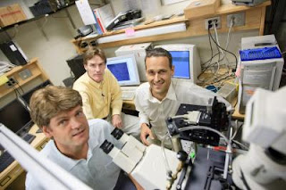
Caption: Wake Forest University physics professors (from left to right) Martin Guthold, Keith Bonin and Jed Macosko work in Guthold's laboratory on development of Lab-on-Bead processing, a novel drug-screening technique with the potential to be 10,000 times faster than current methods.

Credit: Wake Forest University/Ken Bennett, Usage Restrictions: None.
Researchers at Wake Forest University are using nanotechnology to search for new cancer-fighting drugs through a process that could be up to 10,000 times faster than current methods.

The "Lab-on-Bead" process will screen millions of chemicals simultaneously using tiny plastic beads so small that 1,000 of them would fit across a human hair. Each bead carries a separate chemical, which can be identified later if it displays the properties needed to treat cancer cells. One batch of nanoscopic beads can replace the work of thousands of conventional, repetitive laboratory tests.
"This process allows the beads to do the work for you," explains Jed Macosko, project director and assistant professor of physics at Wake Forest. "By working at this scale, we will be able to screen more than a billion possible drug candidates per day as opposed to the current limit of hundreds of thousands per day."

Other members of the research team at Wake Forest include co-principal investigator Martin Guthold, an associate professor of physics, and Keith Bonin, department chair and professor of physics.

Macosko said the team and their collaborators at the University of Waterloo in Ontario, Canada, are developing a device that will automate the Lab-on-Bead process and permit parallel processing to attain faster screening results. The Wake Forest researchers are also working with biotechnologists at Harvard University in Boston and Université Louis Pasteur in Strasbourg, France, which are providing the chemicals being screened for drug candidates. Biotech company NanoMedica has shown interest in commercializing the process. The North Carolina Biotechnology Center, a private, nonprofit corporation funded by the N.C. General Assembly, has provided $75,000 in funding for the project.

Wake Forest's Center for Nanotechnology and Molecular Materials, which maintains ongoing research programs in the areas of health and medicine, energy technologies and synthesis of nanomaterials, will facilitate some elements of Lab-on-Bead development. ###

Contact: Eric F. Frazier frazieef@wfu.edu 336-758-5237 Wake Forest University

Tags: or and

Friday, November 14, 2008

US Senate confirms Clemson University engineering Dean Esin Gulari to National Science Board

Esin Gulari, Clemson University

Caption: Esin Gulari, Credit: Clemson University, Usage Restrictions: None.
The U.S. Senate has confirmed the appointment of Esin Gulari, dean of the College of Engineering and Science at Clemson University, to serve on the National Science Board (NSB). President George W. Bush nominated Gulari for the post along with six other distinguished scientists.

"This is a tremendous honor for me as a scientist and an engineer," said Gulari. "On the NSB, I will be in a unique position to make contributions on a national level.
I hope that my participation will bring distinction to the university and focus a national spotlight on Clemson, and more specifically, the exciting work going on in the College of Engineering and Science."

The National Science Board is an independent body of advisers to both the president and Congress on broad national policy issues related to science and engineering research and education. It also serves as an oversight body for the National Science Foundation. Members are drawn from industry and universities, representing a variety of science and engineering disciplines and geographic areas. Gulari was selected for her preeminence in research, education and public service. She will serve a six-year term to expire in May 2014.

"Congratulations to Dean Gulari," said Clemson President James F. Barker. "The caliber of this appointment to the highest science board in the country is a reflection of her expertise and talent as a scientist. Clemson University could not be more proud."

Gulari is the first woman to serve as dean of Clemson University's College of Engineering and Science and its nearly 5,000 students. The college includes 14 academic departments, 23 undergraduate and 45 graduate degree programs and 11 research centers, including the Clemson University International Center for Automotive Research (CU-ICAR).

Since coming to Clemson in June 2006, Gulari has created two new units within the college. The first is the School of Computing, which has the mission to prepare students for all aspects of computing as part of a universitywide emphasis on information technology and high-performance computing. The aim is to allow for rapid development of emerging, interdisciplinary research and academic programs. The department of engineering and science education is the second unit established and is designed to improve the educational methods and pedagogy of teaching science and engineering at the university level and to reach out to K-12 education with innovative strategies in math, science and engineering.

Prior to becoming dean, Gulari served as professor and chairwoman of the chemical engineering and materials science department at Wayne State University. She has private-sector experience having served as chief technology officer of nanoSEC, a startup company formed to manufacture and market nanocomposites produced using supercritical fluid processing.

From 2000 to 2004, Gulari served at the National Science Foundation, where she was director of the Chemical and Transport Systems Division in the Engineering Directorate, and during most of that time as acting assistant director for the Engineering Directorate.

Other National Science Board nominees include: France Córdova, president, Purdue University; Bud Peterson, chancellor, University of Colorado, Boulder; and Diane L. Souvaine, professor and chairwoman, department of computer science, Tufts University. The following board members were re-nominated to serve a second term: Barry Barish, professor of physics emeritus and director, LIGO Laboratory, California Institute of Technology; Ray Bowen, president emeritus, Texas A&M University; and Douglas Randall, professor and Thomas Jefferson Fellow, University of Missouri, Columbia. ###

Contact: Esin Gulari egulari@clemson.edu 864-656-3202 Clemson University

Tags: or and